Showing posts with label Microcontroller. Show all posts

Digital basic logic gates

Digital basic logic gates, or often also called Boelan logic gates is a digital logic gate will output a logic 0 and 1 corresponds to the input received from each gate depends on the function logic. In the digital basic logic, there are 3 basic logic gates, ie AND gates, OR gates, NOT gates. Third this gate produces 4 next digital logic gates, namely: NAND gates, NOR gates, XOR gates, gate XAND.

AND Logic Gate
AND logic gate has the output formula AB = C, ie when both its inputs are not all the logic 1 output will be logic 0 and when both input logic 1 then the new output is logic 1.

OR Logic Gate
OR logic gate having an output summing function can be formulated A + B = C ie if one input is logic 1 then the output will be logic 1 and when both input logic 0 then the new output will be logic 0.

NOT logic gate
NOT logic gate or often also called inverting logic gates. NOT gate will output a value opposite of the input.

Interface LCD SED 1200 and Mikorokontroler AT89C2051

Microcontroller AT89C2051 is a 20 pin version of the microcontroller AT89C51. Technical interface to microcontroller AT89C51 AT89C2051 and can be prepared very simply. SED 1200 LCD can be used to display 20 letters / numbers very good, quite adequate for displaying telephone numbers and other short message message. As the LCD display in general, SED1200 consists of two parts, namely the LCD panel which consist of many 'points' LCD and a microcontroller attached to the panel and serves to set 'the dots' LCD'd be the letters / numbers that read, as well as functions for communication between the LCD display with another microcontroller using the LCD display. Task LCD display microcontroller users only send ASCII codes to be displayed.

In the data sheet says SED1200 LCD display is compatible with 4-bit microprocessor and 8 bits, this is due to SED1200 only equipped with 4 channels of data (DB0 .. db3) is used to distribute the ASCII code or command to set its SED1200. In terms of ASCII codes and commands are all 8-bit codes, the codes were sent twice, which first shipped is 4 bits are weighted higher (most significant bit - D4 .. D7) and then the remaining 4 bits (D0. . D3). In addition to DB0 .. db3, SED1200 also equipped with CS, WR and A0 such as components that are compatible with the microprocessor, which is somewhat distorted signal CLK lajut which will be discussed further below.

A0 is used to distinguish data that is sent to the SED1200, if A0 = 0 data sent is a command to control the SED1200 and vice versa if A0 = 1 data sent is ASCII code you want to display.

The process of sending data to the SED1200 depicted in Figure 1 can be described as follows:

CS signal is used to activate the process of sending this data, during this process CS activated by voltage level '0 '.
The data will be sent to the SED1200 prepared at DB0 .. db3, as discussed above codes are sent to the SED1200 split into 2 time delivery, this is seen clearly in Figure 1 which describes the delivery of D4 .. D7 .. D0 and subsequent delivery D3.
After the data is ready, WR signal is used as a signal of 'commando' for the SED1200 to retrieve the data on DB0 .. db3. Data collection is exactly what happened at the time of WR changed from '0 'to '1'
Interface to AT89C2051
AT89C51 AT89C2051 is a simplified into a microcontroller which only the legs of 20, a simplification that resulted AT89C2051 not have the legs DB0 .. DB7, P2.0 .. P27, WR, RD and ALE and how many other feet, other than that the instruction MOVX @ DPTR, A can not be used, thus the circuit of Figure 2 at all can not be used for the AT89C2051, and instead made the circuit of Figure 3, in this series and WR DB0 .. db3 replaced with Port 1 and its function is simulated through the program.

SED1200 CLK foot foot connected with P1.7 AT89C2051, SED1200 pulses required to process the received data generated by the program, it is not necessary to provide a special circuit to generate clock.

Cuts Program 2 is a sub-routine to control the SED1200 are connected to the AT89C2051 as shown in Figure 3, before taking the second sub-routine, the data to be sent to the SED1200 had to be prepared in the accumulator A.

Differences sub-routine and KirimASCII KirimPerintah lies in the value A0 at the time of the sub-routine work. Sub-routine KirimPerintah work with A0 = '0 '(line 7), AT89C2051 received data sent as a command to set the SED1200 SED1200 work. Sub-routine KirimASCII work with A0 = '1 '(line 11), received the data sent AT89C2051 SED1200 as ASCII code to be displayed
Throughout the process activated by the CS data transmission voltage level '0 'is done in line 13 and in his re-nonaktip on line 19.
Data in the accumulator A is sent byte-by-half-byte half twice, first sent A4 .. A7 (lines 15 and 16) then sent A0 .. A3 (lines 17 and 18).
Given AT89C2051 no ALE signal instead row 22 to be raised 16 to 25 clock pulses required by the CLK SED1200. 16 pulse is generated after A.0 .. A.3 sent to the SED1200, out of the sub-routine is SED1200 is ready to receive data again.
Line 29 to 36 Discount Program 2 simulates line 21 Discount Program 1, in line 29 feet WR SED1200 in zero out, lines 30 to 35 send to DB0 A0 .. A3 .. db3 (P1.0 .. P1.3) without changing the other signals are already in Port 1. In line 36 WR returned to '1 ', then that information on DB0 .. db3 taken by SED1200.
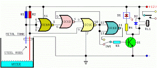
Automatic Water Pump Controller

Automatic water pump controller is a series of functions to control the water pump otamatis in a reservoir or water storage. As the water level sensor made with a metal plate mounted on the reservoir or water tank, with a sensor in the short to create the top level and a detection sensor for detecting long again made the lower level and ground lines connected to the bottom of reservoirs or reservoir. The series of automatic water pump controller is designed with 2 inputs NOR by 4 pieces and relay that is activated by the transistor. Automatic water pump circuit requires +12 VDC voltage source and can be used to control the water pump is connected to AC power jalringan. Here is the complete series of pictures.

Series Automatic Water Pump Controller


Sign Component Automatic Water Pump Controller
R1 = 15K
R2 = 15K
R3 = 10K
R4 = 1K
D1 = LED
D2 = 1N4148
Q1 = BC337
IC1 = 4001
SW = SPDT Switches
Relay RL1 = 12V

The working principle series of automatic water pump controller above is. At the time the water level is below both sensors, the output IC1C (pin 10) will be LOW, Kemudin when the water began to touch the lower level sensor, the output IC1C (pin10) remains LOW until the water touches the sensor level above, then the output IC1C (pin 10) going HIGH and active relay through Q1 and turn on the water pump to meguras reservoir. At the muli down and water level sensors for water untouched MKA IC1C output (pin 10) remains HIGH until the new water untouched semuasensor IC1C output (pin 10) LOW and water pump died. The series of automatic water pump controller is equipped with SW1 which serves to reverse the logic of drains (the output of IC1C) and the concept of water supplied (output dri IC1D). When SW1 is connected to IC1D the water pump will turn on when the water does not touch all the sensors and will die when all the sensors tesentuh water. Automatic water pump controller can be used to fill or drain the water according to which mode is selected via SW1.

Egg incubator comtrol list Program

List Program Temperature Controller AT89C2051 egg incubator is a program used to control the temperature control device incubator Egg With AT89C2051 which details a series of articles exist on Temperature Controller With AT89C2051. Many requests are asking for the program lists a series Temperature Controller AT89C2051 egg incubators. Hopefully with the upload list of programs from a series Temperature Controller AT89C2051 egg incubators can help and give inspiration to all who are looking teman2 reference to the construction of the Temperature Controller egg incubators. Temperature Controller program listings AT89C2051 Egg incubators that I uploaded are still many shortcomings, so it can be developed more to get better. Following the program listings.

Universal PIC Programers

The series of Universal PIC Programmer can be used with software IC-Prog 1:05. Universal PIC programmer circuit is very simple with BC337 transistor 1 pieces, 2 pieces of IC regulators 7805 and 7808 as well as some components of passive supporters. Universal PIC Programmer series can be supplied with 2 pieces of 9V batteries. For communication with computer circuit Universal PIC Programmer uses a serial RS232 port of computer. Then for the PIC to be programmed provided 5 lanes for the PIC that is DATA, Clock, Vpp, Vcc and Ground. For more details, can be directly seen in the figure below.

Universal PIC Programers

The series of Universal PIC Programmer can be used to program the PIC family of 16F84A series, 12C509, 16C765 and the other. Hopefully this series of Universal PIC Programmer can help for friends who want to make PIC programmer

PIC Volt and Amere Meter Circuits

Volt meter and ampere meter with PIC can be used to measure voltage and current at the same time. The series of volt meter and ampere meter with PIC uses a PIC16F876A as a data processor voltage and current are measured. This circuit uses a LCD viewer 16 × 2, which is used for displaying data voltage and current measurements. In the article volt meter and ampere meter with PIC is to be discussed is limited to devices faucet only. For more details can be seen from the image sequence volt meter and ampere meter with PIC below.


In the circuit volt meter and ampere meter with PIC above used 3 pieces of buttons for setting Calibration measurement data. The circuit is basically working with the source voltage 5VDC.

Serial to Parallel circuits

In creating an electronic device using a microcontroller, we often faced with shortages in ports for line I / O or LCD viewer. In the article series LCD with 74HC595 Serial To this there is a solution to overcome the lack of ports or pins of the microcontroller is to convert the parallel bus system such as the LCD into a serial sequence To Serial LCD with 74HC595 this. The series of LCD Serial To change the system of parallel bus into a serial LCD IC 74HC595 premises. 74HC595 IC on circuit Serial To this LCD is a digital IC that it functions as a serial to parallel shift register is equipped with a latch. With the functions of the IC 74HC595 parallel LCD bus system in enter in great numbers have turned into a serial of microcontroller and be a series of Serial LCD with 74HC595 for this. Now with a range Serial To LCD with 74HC595 for the microcontroller is expected no more stories lack the pin / port of the microcontroller in the manufacture of electronics equipment.
Serial to Parallel circuits


The series of Serial Line Specification For LCD with 74HC595
  • Clock as input clock of the microcontroller
  • Data as input data for the LCD display
  • Enable is the read data selector LCD mode or Disable
  • LED is a path to control LED LCD baground
  • Potensimeter on the LCD serves to adjust the LCD display bright
Hopefully helpful and inspiring in the case of lack of lane / port microcontroller to the viewer data.